6" InP 기능으로 포토닉스에 전례 없는 확장 제공
바카라 카지노는 고속 반도체 이상을 위한 세계 최초의 6인치 InP 확장 가능 웨이퍼 팹을 출시했습니다.
2024년 12월 9일 작성자:일관적인

갑자기 InP(인듐 인화물) 웨이퍼의 미래가 훨씬 더 밝아 보입니다. InP 웨이퍼가 통신 분야 및 그 이상 분야의 고속 광자 장치를 위한 강력한 솔루션을 제공한다는 것은 비밀이 아닙니다. 하지만 최신 이정표는요?
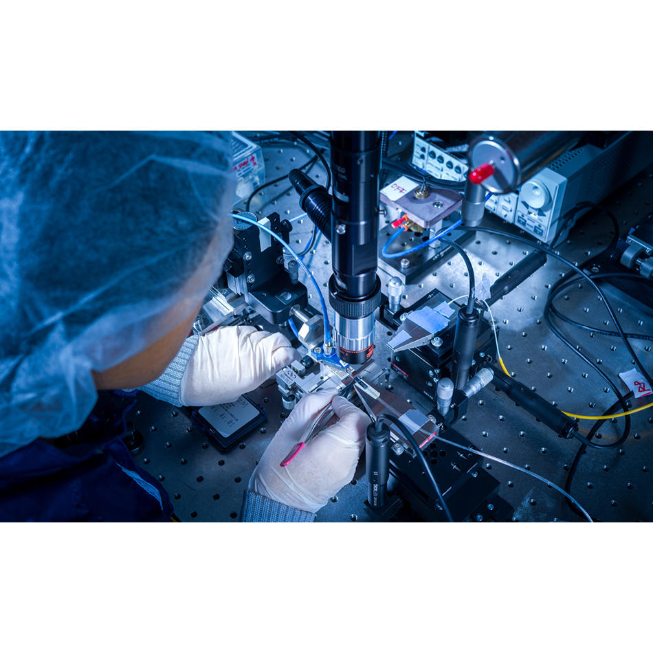
바카라 카지노가 최근 발표함텍사스의 Sherman과 스웨덴의 Järfälla 웨이퍼 공장에서 InP 웨이퍼 제조를 위한 세계 최초의 6인치 기능을 선보였습니다.
전반적으로 6인치 인듐 인화물 웨이퍼로의 전환은 반도체 산업의 중요한 발전을 나타냅니다. 다음으로 이러한 전환의 몇 가지 주요 이유를 살펴보겠습니다.
더 큰 InP 웨이퍼로 패러다임 전환
비용 효율적입니다. 믿을 수 있는. 고속. 지속 가능한. 이러한 높은 수준의 장점 외에도 당사의 최신 6인치 제품과 같은 더 큰 인화인듐(InP) 웨이퍼는 반도체 기술 발전에 중요한 몇 가지 중요한 이점을 제공합니다.
생산 능력 증가.더 큰 웨이퍼는 웨이퍼당 더 많은 장치를 허용하여 AI 상호 연결, 데이터 통신, 통신, 자동차, 산업 및 소비자와 같은 성장하는 시장에서 급격히 증가하는 광 장치 수요를 충족할 수 있도록 팹의 전체 생산 용량을 확장하여 경쟁력과 수익성을 향상시킬 수 있습니다.
다이 비용 감소.6인치 웨이퍼로 전환하면 바카라 카지노는 고용량, 보다 효율적인 자동화 공정 도구를 활용하여 설치 공간을 확장하지 않고도 팹의 용량을 늘리고 웨이퍼당 인건비를 낮출 수 있습니다. 이러한 개선으로 다이 비용이 60% 이상 절감되었습니다.
향상된 효율성.더 큰 웨이퍼 크기는 향상된 균일성을 제공하여 더 나은 수율을 제공합니다. 또한 웨이퍼 인증과 같은 활동으로 인한 다이당 간접비도 절감됩니다.
미래 애플리케이션.6인치 InP 웨이퍼 제조는 다음을 포함하여 수요가 많은 사례에 대한 생산 능력을 허용합니다.
- 일관된 광통신:다양한 고속 데이터 전송 애플리케이션에 사용됨
- 데이터콤 송수신기:데이터 센터 및 통신 네트워크에 필수
- AI 상호 연결:인공지능 애플리케이션의 새로운 혁신과 증가하는 수요 지원
- 고급 감지:소비자 전자제품, 웨어러블 기기, 의료 기기, 자동차 애플리케이션 등에 사용
- 6G 무선 및 위성 통신 네트워크:InP 웨이퍼는 이번 10년 후반에 무선 기술에서 중요한 역할을 할 것입니다.
보다 지속 가능한 옵션.생산의 효율성이 증가함에 따라 자원에 대한 영향은 물론 지속 가능성도 향상됩니다. 2023년 Deloitte 연구에 따르면 반도체 산업에서 제조(예: 대형 InP 웨이퍼)의 발전은 에너지 집약도의 전반적인 감소를 지원하는 데 도움이 될 수 있습니다.
트랜시버의 미래에 대한 우리의 역할
고성능 주력 장치인 일관성 있는 송수신기는 마라톤 선수와 같습니다. 그들은 수천 킬로미터를 질주하며 단일 파장에서 초당 최대 800기가비트의 속도로 데이터를 전달합니다. 이러한 애플리케이션에 대한 수요는 더욱 강력해질 뿐 아니라 전문 지식, 기술 및 제조 역량의 통합도 마찬가지입니다.

바카라 카지노 InP 광자 집적 회로는 복잡한 변조 파형을 인코딩 및 디코딩하는 고밀도 다중화 시스템에 필요한 레이저 파장을 지원합니다. 궁극적으로 이 기능을 통해 이러한 파장은 장거리 네트워크 등을 통해 고용량 데이터를 전달할 수 있습니다.
데이터콤 및 AI 애플리케이션에서 InP 기반 외부 변조 레이저와 고출력 CW 소스 레이저는 대규모 데이터 센터 및 기계 학습 클러스터를 위한 트랜시버 솔루션의 신속한 배포를 가능하게 합니다. 이러한 애플리케이션에 대한 수요가 빠르게 확장하려면 이에 맞춰 확장할 수 있는 팹 역량이 필요하며, 6인치 웨이퍼 크기로의 전환이 이를 가능하게 할 것입니다.
세계적 수준의 품질, 성능, 출시 기간 및 비용 이점은 200G EML(전기 흡수 변조 레이저), DFB-MZ(통합 Mach-Zehnder 변조기)가 포함된 200G 분산 피드백 레이저와 같이 새로운 6인치 InP 플랫폼에서 마이그레이션하는 여러 기존 제품을 포함하여 바카라 카지노의 광범위한 제품 제공 포트폴리오의 핵심 요소입니다. 100G EML, 실리콘 포토닉스 애플리케이션을 위한 고속 광검출기 및 CW 레이저.
미래 혁신 및 요구 사항과 보조를 맞춰
레이저, 감지기 및 전자 장치에 대한 수요가 산업과 응용 분야 전반에 걸쳐 계속 증가함에 따라 바카라 카지노는 전반적으로 더 큰 웨이퍼 크기의 이점을 최대한 활용하기 위해 3인치 InP에서 6인치 InP로 생산을 발전시키는 과정에 있습니다.
이 중요한 전환은 진화하는 시장의 요구에 필수적이며 귀하의 조직이 경쟁 우위를 유지하는 데 도움이 될 수 있습니다. 수십 년 동안 트랜시버 분야의 선두주자였던 바카라 카지노는 혁신과 변화하는 시장 요구에 발맞춰 새로운 요구 사항을 충족하기 위해 협력할 것입니다.
자세히 알아보기일관된 인듐 인화물(InP) 웨이퍼 제조.