더 나은 열 관리로 반도체 패키징 개선
SiC와 같은 고급 소재는 오늘날의 더 얇은 마이크로전자 부품에 필요한 새로운 조립 방법을 가능하게 합니다.
2023년 12월 20일 by일관적인

초소형 회로가 축소됨에 따라 이를 제조하는 데 사용되는 모든 공정은 더 작고 얇은 회로로 작동하고 더 높은 정밀도를 제공하기 위해 재조정되거나 교체되어야 합니다. 이는 특히 "고급 포장"에 해당됩니다. 이는 개별 집적 회로("다이"라고 함)를 장착하고 기판이나 회로 기판에 전기적으로 연결한 다음 밀봉하는 생산 단계입니다.
플립칩 기본사항
널리 사용되는 고급 패키징 기술 중 하나는 "플립 칩"입니다. 이 방법은 와이어 본딩과 같은 기존 방법에 비해 몇 가지 장점을 제공하기 때문에 지난 10년 동안 점점 인기를 얻었습니다. 이러한 이점에는 비용 절감, 패키징 밀도 향상, 신뢰성 향상 등이 포함됩니다.
플립 칩용 회로를 준비하기 위해 전도성 물질(일반적으로 납땜 또는 금)의 작은 범프가 먼저 반도체 웨이퍼 상단 표면의 전도성 패드에 증착됩니다. 그런 다음 웨이퍼를 개별 칩으로 절단합니다(다이 싱귤레이션이라고 함).
다음으로 개별 다이를 집어 올려 접촉면이 아래를 향하도록 회전시킨 후 장착할 기판 위에 위치시킵니다. 이 기판은 가장 일반적으로 인쇄 회로 기판입니다. 칩은 칩의 범프가 기판의 해당 전도성 패드(위를 향함)와 일치하도록 매우 정밀하게 정렬됩니다. 칩 범프는 기판 패드와 접촉하게 됩니다.
이 어셈블리는 오븐에 넣어 땜납(또는 범프를 구성하는 모든 것)의 녹는점 이상으로 가열됩니다. 솔더는 녹아서 다이와 기판 모두의 전도성 패드에 달라붙어 "리플로우"됩니다. 마지막으로 오븐이 냉각되고 솔더가 응고되어 칩과 기판 사이에 전기적, 기계적 결합이 형성됩니다.
열압착 접합 – 얇은 다이를 위한 솔루션
플립칩 공정은 IC와 기판이 모두 얇아지고 솔더 범프 크기와 이들 사이의 간격(피치라고 함)이 100μm 미만으로 줄어들면서 문제에 직면하기 시작합니다. 특히, 가열 주기는 IC와 기판에 변형을 일으킬 수 있습니다. 이는 가열 주기 동안 이러한 구성 요소 전체의 온도 구배와 다양한 부품 간의 열팽창 계수(CTE) 불일치로 인해 발생할 수 있습니다.
부품 변형이 충분히 크면 다이와 기판 사이에 정렬 불량이 발생할 수 있습니다. 이로 인해 개방 회로(연결 없음)가 발생하거나 경우에 따라 단락(납땜 볼 브리징)이 발생할 수도 있습니다.
열압착 접합(TCB)은 플립칩의 기능을 확장하기 위해 특별히 개발된 기술입니다. 특히 TCB는 얇은 다이의 대량 칩 부착을 수행하는 보다 안정적인 방법을 제공합니다.
기존 플립 칩 본딩과 TCB의 차이점은 후자가 매우 높은 정밀도로 전체 작업 중에 다이와 기판의 온도, 가해진 힘, 위치 및 방향을 적극적으로 모니터링하고 제어한다는 것입니다. 프로세스의 각 단계는 다음 단계로 넘어가기 전에 확인됩니다. 이러한 모든 제어를 통해 더욱 우수하고 안정적인 결합과 단위 간 일관성이 향상됩니다.
이 모든 것을 달성하기 위해 사용된 TCB 시스템의 주요 요소가 그림에 표시되어 있습니다. 여기에는 1μm의 정밀도로 다이를 수직으로 배치할 수 있는 에어 베어링 축의 선형 서보 모터가 포함됩니다. 칩과 다이의 동일 평면성을 유지하기 위해 각도 위치 지정을 위한 팁-틸트 스테이지도 있습니다. 히터와 쿨러 모두 다이의 온도와 온도가 증가하거나 감소하는 속도를 정밀하게 제어합니다. 이 구성 요소 스택의 맨 아래에는 다이 자체를 고정하는 진공 척 또는 노즐이 있습니다. 그리고 일련의 센서가 내장되어 전체 작업 중에 온도, 가해진 힘, 다이와 기판의 위치 및 방향을 지속적으로 모니터링합니다.

열 압축 접합 시스템에는 다이와 기판의 위치와 방향을 지정하는 단계, 온도를 제어하는 히터와 쿨러, 다이를 고정하는 진공 노즐, 프로세스를 모니터링하고 제어하는 다양한 변환기와 비전 시스템(표시되지 않음)이 포함됩니다.
TCB 프로세스는 기존 플립 칩과 동일하게 시작됩니다. 즉, 솔더 범프를 사용하여 다이를 준비한다. 그런 다음 다이를 집어 올려 기판과 정렬한 다음 범프가 기판과 접촉할 때까지 아래로 내립니다. 그 후, 가열 및 다이 이동 사이클이 시작됩니다.
땜납이 녹으면서 다이는 먼저 기판 쪽으로 이동한 다음 기판에서 약간 멀어지고 마지막으로 다시 기판 쪽으로 이동합니다. 온도와 가해지는 힘도 다양합니다. 이 모든 것이 다이와 기판 간의 우수한 정렬 및 결합, 균일한 납땜 접합 높이, 결함 없는 연결을 보장합니다.

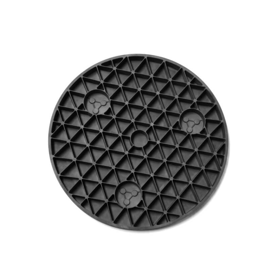
바카라 카지노는 TCB 노즐용 재료 및 완성 부품을 수직적으로 통합한 생산업체입니다. 우리는 다양한 크기와 모양, 그리고 이 4H SiC 부품과 같은 내부 기능을 갖춘 노즐을 제작할 수 있습니다.
노즐용 고급 소재
TCB 시스템의 스테이지, 열 장치 및 센서 외에 또 다른 중요한 요소는 노즐입니다. 세 가지 주요 기능을 제공합니다. 첫째, 공기 흐름을 위한 다양한 구멍이나 채널이 포함되어 있어 진공 척 역할을 할 수 있습니다. 둘째, 공정 전반에 걸쳐 다이의 평탄도를 유지합니다(진공이 부품을 표면에 단단히 고정시키기 때문입니다). 마지막으로 TCB 시스템의 가열 및 냉각 요소가 다이의 온도를 변화시킬 수 있도록 열을 전도합니다.
이러한 요구 사항을 충족하려면 매우 부드럽고 평평한 부품으로 만들 수 있는 기계적으로 견고한 재료로 이상적인 노즐을 제작해야 합니다. 이는 다이에 가해지는 힘이 변하더라도 프로세스 전반에 걸쳐 다이를 단단히 고정하고 평평하게 유지하는 데 필요합니다.
또한 노즐 재료는 열 전도성이 높아야 합니다. 이는 히터와 쿨러에 의해 시작된 온도 변화가 다이를 통해 빠르게 전달되도록 보장합니다. 다이의 온도를 정밀하게 제어하고 이를 빠르게 열 순환시키는 능력은 프로세스 성공과 전체 택트 타임 최소화의 핵심입니다.
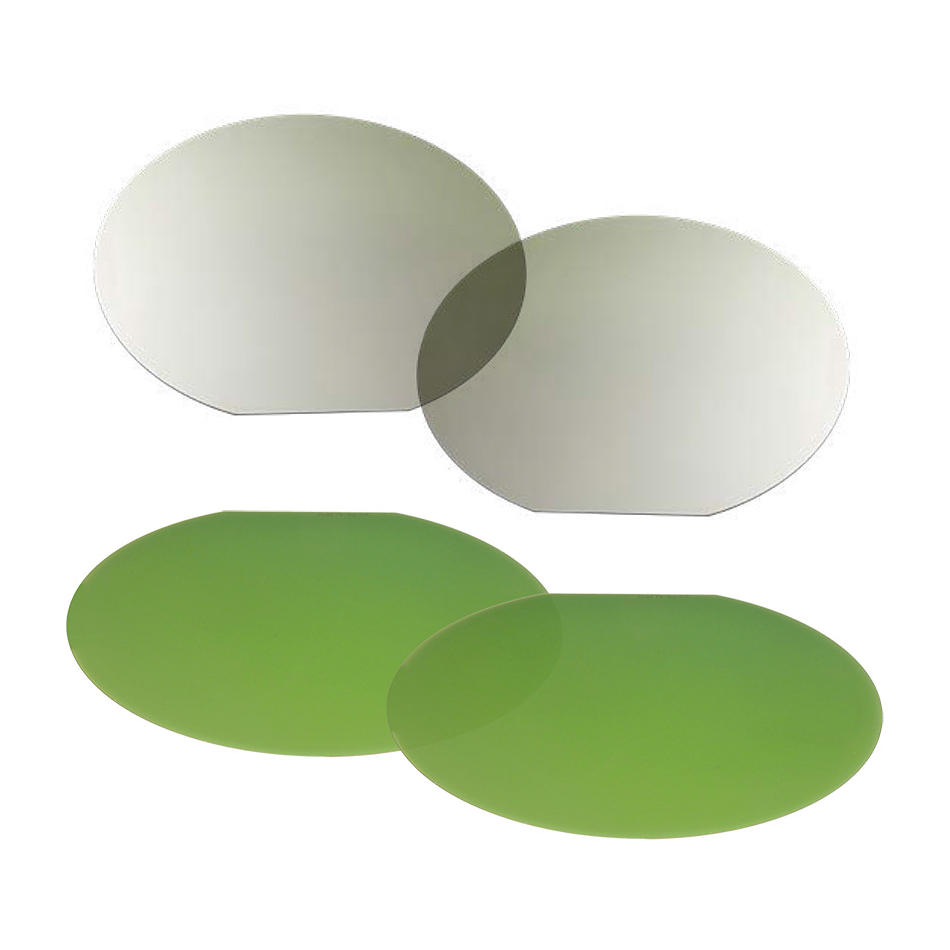
이러한 모든 요구 사항을 충족하는 재료는 거의 없지만 바카라 카지노는 세 가지 다른 재료를 생산하고 그 중 어느 것에서든 완성된 TCB 노즐을 제작할 수 있습니다. 이들은반응 결합 탄화규소(SiC),단결정 SiC및다결정 다이아몬드. 각 제품에는 고유한 특성과 장점이 있으며 표에 요약되어 있습니다.
재료 |
열전도도 |
표면 거칠기 |
광 투과형 |
전기 절연체 |
비용 |
반응 결합 SiC |
255W/m-K |
< 25nm |
아니요 |
아니요 |
낮음 |
단결정 SiC |
370W/m-K |
< 2nm |
예 |
4H: 아니요 6H: 예 |
중간 |
다결정 다이아몬드 |
2200W/m-K |
< 10nm |
예 |
예 |
높음 |
이 모든 물질은 다른 물질에 비해 높은 열 전도성을 제공합니다. 다이아몬드는 모든 물질 중 가장 높은 열 전도성을 가지고 있습니다. 반응 결합 SiC의 주요 특징 중 하나는 관통 구멍이나 내부 채널이 필요한 모든 것을 쉽게 생산할 수 있다는 것입니다. 또한 레이저 가공을 통해 매우 높은 평탄도와 낮은 표면 거칠기를 달성할 수 있습니다.
다이아몬드와 단결정 SiC의 장점은 가시광선과 근적외선 영역에서 투과성이 있다는 것입니다. 이를 통해 최종 부품의 평탄도, 두께 및 평행도를 측정하는 데 광범위한 측정 기술을 사용할 수 있으므로 더 높은 정밀도의 제작이 가능해집니다.
다결정 다이아몬드와 6H 단결정 SiC는 전기 절연체입니다. 이 속성은 정전기 방전(ESD)으로 인한 손상으로부터 반도체 다이를 보호하는 등 여러 가지 이유로 유용할 수 있습니다.
이 세 가지 재료로 제작된 노즐의 가격에도 차이가 있습니다. 노즐은 주기적으로 교체되는 소모품이기 때문에 이는 중요합니다.
바카라 카지노는 수직 통합형 TCB 노즐 제조업체입니다. 우리는 자체 재료를 재배하는 것부터 시작하여 완성된 부품을 생산하는 과정까지 진행합니다. 우리 제조 능력의 핵심 구성 요소는 매우 평평한 표면을 생성하는 능력이며, 우리는 이러한 평탄도를 검증하기 위한 광범위한 계측 장비를 보유하고 있습니다.
자세히 알아보기반응 결합 탄화규소(SiC),단결정 SiC및다결정 다이아몬드바카라 카지노에서.